Back-Illuminated CMOS (BI CMOS), also known as BackSide Illumination CMOS (BSI CMOS), is commonly associated with small imaging devices like smartphones. Nowadays, the main cameras in most smartphones use either back-illuminated or stacked CMOS sensors.
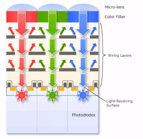
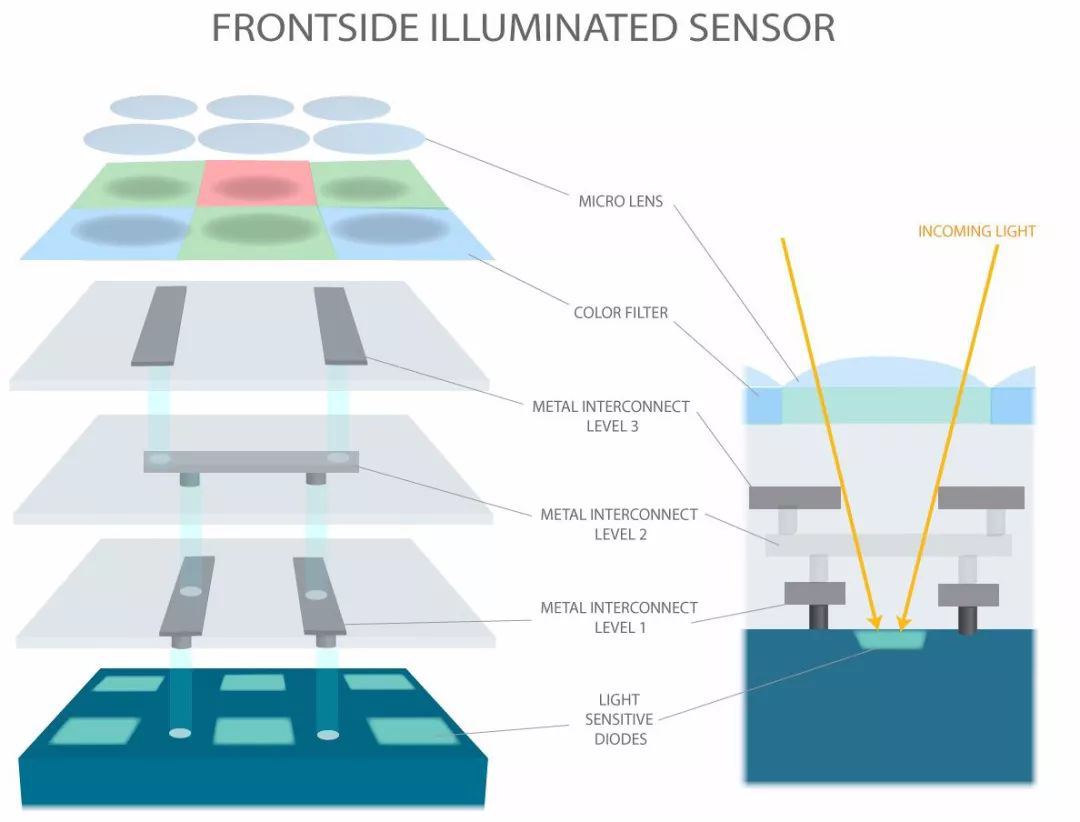
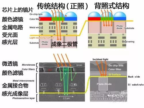
To understand the significance of "back" in back-illuminated CMOS, it's essential to first grasp the structure of traditional CMOS—front-illuminated (FSI). In the traditional FSI structure, from top to bottom, there are micro-lenses, color filters, wiring layers, and photodiodes.
In the FSI structure, the circuitry occupies significant space, leaving less room for photodiodes, resulting in reduced light collection. This limitation impacts image quality, particularly noticeable in high ISO settings with increased noise and artifacts.
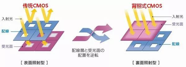
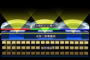
Back-illuminated CMOS addresses these limitations by reversing the positions of the metal wiring layer and the photodiodes. In this configuration, light encounters minimal obstruction and interference, leading to higher light utilization efficiency and improved image quality, especially in low-light conditions.
The development of back-illuminated CMOS has seen significant milestones:
- In the 1990s, the concept of back-illumination was proposed but faced challenges in mass production due to high manufacturing requirements.
- In 2007, OmniVision showcased BSI CMOS samples.
- In February 2009, Sony achieved mass production of BSI CMOS and registered the Exmor R trademark. Products featuring Exmor R CMOS were introduced, including camcorders and digital cameras.
- In October 2011, the primary camera of the Apple iPhone 4S adopted Sony-produced BSI CMOS.
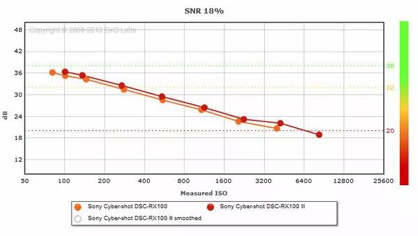
- In June 2013, Sony launched the RX100 II digital camera with a 1-inch BSI CMOS sensor.
- In June 2015, Sony introduced the A7RII mirrorless camera featuring a full-frame BSI CMOS sensor.
The characteristics of back-illuminated CMOS sensors benefit from advancements in manufacturing processes, particularly in two aspects:
- Improved performance of micro-lenses on the sensor surface ensures that incident light angles are closer to perpendicular, reducing undesirable effects like dispersion and glare.
- Despite large pixel sizes, back-illuminated CMOS sensors maintain high-speed processing capabilities compared to CCD sensors. Each pixel in a CMOS sensor converts charge into voltage data, offering significant potential for improving frame rates without increasing noise.
These advantages are not unique to back-illuminated CMOS sensors but are commonly found in modern CMOS sensors. As a result, the widespread adoption of CMOS sensors in digital cameras reflects their ability to deliver high pixel counts and fast performance, influencing consumer preferences.
FALenses Technology specializes in providing machine vision core hardware. You can go to the official website of FALenses Technology at https://www.falenses.com/ for more information.