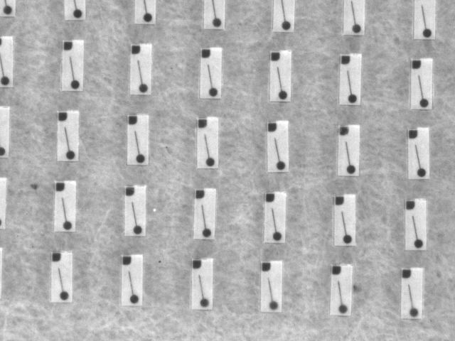
Detection of Crystal Lattice Inside the Crystal Plate
Detection Content: Detection of Crystal Lattice Inside the Crystal Plate
Light Source Used: Point Light Source
Analysis: Microscopic crystal element images taken with a point light source and microscope lens exhibit black features with a white background, showing clear contrast; moreover, the light is uniform.
Industry Overview
The application of machine vision in the semiconductor industry has become increasingly common, with its scope expanding to encompass the detection and measurement of various aspects such as semiconductor appearance defects, dimensions, quantities, flatness, spacing, positioning, calibration, solder joint quality, and curvature.
Detection content includes:
- Inspection of electronic component appearance
- Inspection of SMD (Surface Mount Device) products
- Inspection of silicon wafer appearance
- Inspection of IC (Integrated Circuit) chips
- Inspection of flatness in electronic connectors
Challenges in illumination:
The diversity of product forms, high precision detection requirements, and the fact that product characteristics are not always obvious due to materials and manufacturing processes, result in high demands for illumination.