Global Agents Wanted! Join us to share market opportunities. Comprehensive training, technical support, and attractive incentives provided. Act now for a brilliant future! Contact email: partners@falenses.com
March 19, 2024 Beijing time, NVIDIA held its annual NVIDIA GTC keynote speech again. NVIDIA CEO Huang Renxun shared the breakthroughs of the new generation of AI through this speech, and also allowed the audience to witness another moment of AI transformation.
Huang Renxun, dressed in a familiar leather jacket, is naturally the protagonist of this speech. "There is no conference in the world with such diverse researchers, including a large number of life sciences, healthcare, retail, logistics companies, and so on." He said, "Global companies worth $10 trillion are gathered at GTC."
Huang Renxun said, "We have reached a critical point and we need a new way of computing... Accelerating computing is a huge acceleration. All partners require higher power and efficiency, so what can Nvidia do?"
The subsequent appearance was the Blackwell B200, a larger GPU named after David Harold Blackwell, a mathematician specializing in game theory and statistics, and the first black scholar to be selected for the National Academy of Sciences in the United States.
According to NVIDIA, the size of the B200 is twice that of the "Artificial Intelligence Superchip" Hopper, integrating 208 billion transistors. It is manufactured using a customized two mask extreme N4P TSMC process, and the GPU chip is connected to the chip link via 10TBps to form a single GPU.
The launch of B200 continues NVIDIA's GPU dominance after H100, and currently, there is still no company that can shake its position. This is the return it should have for the past decade of deep cultivation.
But you can notice a small detail, Nvidia has finally abandoned single chip design and turned to multi chip design. The reason is also simple. The B200 adopts TSMC's improved version of N4P process, without significant upgrades in transistor density, while the H100 is already a full mask size chip - its chip size is 814 mm2, with a theoretical maximum of 858 mm2. In this situation, it seems easy to understand the switch to dual chips.
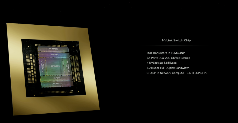
In addition, Nvidia is no longer satisfied with selling individual chips, but instead sells a complete system, the Nvidia B200 NVL72, which contains 600000 parts and weighs 1361 kilograms, and may become a new darling of AI companies.
It can be said that Nvidia has firmly grasped the gold of the AI industry next year through B200 and remains the undisputed king in this field.
FALenses Technology specializes in providing machine vision core hardware. You can go to the official website of FALenses Technology at https://www.falenses.com/for more information.